I had a system with a MVP backplane, but a flaky CPU board set. I also had a spare microVP card. Officially, Wang said the microVP was not compatible with traditional MVP backplanes and would require a new chassis, though the I/O cards were compatible.

After studying the microVP backplane connector pinout and the MVP backplane signal connections, I came up with a small backplane wiring change which allows using the microVP and CS/386 CPU cards in the modified MVP backplane. Unfortunately, the wires would need to be removed to go back to a normal MVP card set.
First, it should be noted there are at least two types of MVP backplanes. The original one had room for four data memory cards (as at the time the DRAM density was low and it required four cards to build out a 128KB system). The later MVP backplane was designed for the "MVP-C" systems, which allowed up to 512KB of RAM and 64K words of microcode. These had one external data RAM controller and two Data Mem slots, and two Control Mem slots. There were also some backplane wiring changes to allow the CPU to address the extra memory.
The change proposed here should be compatible with both types of backplanes, though it has been tested only on the MVP-C style backplane.
Below, the name "IO" corresponds to the I/O expansion slot closest to the CPU cards. "REG" refers to the CPU slot closest to the I/O slots, and holds the CPU registers (typically a 6793 card). "ALU" is the CPU card adjacent to the REG card (typically a 6792 card).
Following the Wang engineering convention, backplane pins are given in the form "X/Y", where X is the pin of the connector, and Y is the connector number (1, 2, or 3). "1" is towards the top of the backplane, and is the shortest of the three connectors in a given slot. The pin-of-edge naming convention is such that the fingers on the same side as the components are named A-S for connector 1 and A-Z for the other two slots; the fingers on the rear of the board are numbered 1-15 on connector 1 and 1-22 on connectors 2 and 3.
- Remove all the cards from the system.
- Remove the pan covering the backplane.
- Make sure you understand the naming convention of the 6798 backplane connectors, especially take into account you are looking at the rear view of the system.
- Bring !PRMS (one of the resets) to the "REG" slot. Do this by running a wire from IO 3/3 to REG 19/2.
- The ALU card normally drives the IOCLK signal to the IO slots. The microVP generates this clock, but the REG slot in the MVP isn't connected to it, so run a jumper wire from REG N/1 to IO L/3.
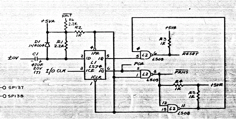
- The reset circuit on the MVP needs a clock input, which is normally !T2 from the ALU card. Instead, we use the IOCLK signal (as does the microVP) to drive the flop. To drive !T2 with IOCLK, run a short jump wire from REG N/1 to ALU 12/1.
- Double check your work.
- Put the microVP or CS/386 card into the REG slot, formerly occupied by the 6793 card.
- Put the I/O cards back in the system.
- Cross your fingers and power it up.
- If all is well, put the pan back over the backplane.
After making the wiring changes, it should look like the picture below (click for a higher resolution view). Ignore the yellow wires running off to the left; the green wires and the short bare wire correspond to the directions given above. Note in a couple cases, rather than soldering to the named pin, the wire was soldered to a through-hole connected to the named pin.

The diagrams below why a clock needs to be run to the reset circuit. Note that the reset circuit in the MVP uses !T2, while the microVP uses IOCLK to advance the 7474 flip-flop.