
The 2200 CPU consists of a backplane constructed of a large printed circuit board (not wire-wrapped) with many point to point connections between the various boards. Each slot in the backplane has a specific function and only one type of card can be inserted in a given slot. At the very end of the backplane is the I/O bus. Different versions of the motherboard were produced with different numbers of I/O slots (five to eleven).
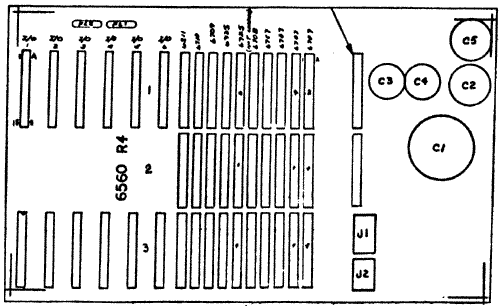
While the CPU slots have three I/O connectors (30 pins each, arranged as 15 double sided positions), the I/O slots have only two connectors (#1 and #3). Interestingly, the I/O cards have three edge connectors, but the middle one doesn't plug into anything. This extra connector was used to provide access to test points for validation and debug, but it goes unused in a normal system. Figure 1, below, is an image of the 2200S/T motherboard. To the right is the linear power supply; in the middle are the ten slots holding the memory and CPU logic. To the left are six I/O slots.
Figure 1: 2200S Backplane
I/O Card Pin Assignment (link)
The I/O bus is a true bus -- all slots are identical, with a common bus trace running to corresponding pins of all the I/O slots. The I/O bus uses normal TTL outputs for signals driven by the CPU and open collector TTL signaling for signals received by the CPU. The pull-up termination appears on the I/O control logic board.
| Pin | Name | Pin | Name |
|---|---|---|---|
| 11 | +15VU1 | A1 | +15VU1 |
| 21 | +5VR LOGIC | B1 | +5VR LOGIC |
| 31 | 0V | C1 | 0V |
| 41 | n/c | D1 | !AB1 |
| 51 | !AB2 | E1 | !AB4 |
| 61 | !AB3 | F1 | !AB5 |
| 71 | n/c | H1 | !OBS |
| 81 | n/c | J1 | !ABS |
| 91 | n/c3 | K1 | !HALT (o.c.) |
| 101 | n/c | L1 | !IB7 (o.c.) |
| 111 | n/c | M1 | !IB8 (o.c.) |
| 121 | n/c | N1 | !IB5 (o.c.) |
| 131 | n/c | P1 | !IB6 (o.c.) |
| 141 | !IB3 (o.c.) | R1 | !IB4 (o.c.) |
| 151 | !IB1 (o.c.) | S1 | !IB2 (o.c.) |
| Pin | Name | Pin | Name |
|---|---|---|---|
| 13 | !IBS (o.c.) | A3 | !OB1 |
| 23 | !IB9 (o.c.) | B3 | !OB2 |
| 33 | !PRMS | C3 | !OB3 |
| 43 | !CPB | D3 | !OB4 |
| 53 | !CBS | E3 | !OB8 |
| 63 | !AB6 | F3 | !OB7 |
| 73 | !AB7 | H3 | !OB6 |
| 83 | !AB8 | J3 | !OB5 |
| 93 | +8VU | K3 | !RB (o.c.) |
| 103 | -15VU2 | L3 | CKL4 |
| 113 | CH. GND | M3 | CH. GND |
| 123 | -12VR | N3 | -12VR |
| 133 | 0V | P3 | 0V |
| 143 | +5 VR LOGIC | R3 | +5VR LOGIC |
| 153 | +12VR | S3 | +12VR |
Notes:
- The suffix "VU" means unregulated voltage.
- The suffix "VR" means regulated voltage.
- The comment "(o.c.)" indicates an open-collector signal with a 1K-ohm pull-up.
- On the 2200S/T and 2200VP motherboards, +15VU is labeled as +18VU.
- On the 2200S/T motherboard, -15VU is labeled as -18VU and is a no-connect on the 2200VP.
- On the 2200S/T motherboard, 91 is labeled as !ERG.
However, the signal is used to preset a status flop that doesn't get used. - On the 2200VP motherboard, L3 is labeled "I/O CLK" instead of "CKL".
CPU Interface (link)
Figure 2 shows the relevant portion of the 6311 I/O controller card, used by the 2200 CPU.
The K register is the architecturally visible register pair known as KH (high 4 bits) and KL (low 4 bits) in the 2200 CPU, whereas it is a simple 8b wide register in the VP architecture. Any data read from or written to an I/O device, and the address of any device selected must go through the K register. The details of when the CPU or I/O device gets to load the K register will be described later.
The AB register is not architecturally visible in that the register can't be read and it is indirectly written. The contents of the K register get latched by the AB register when the CPU performs a CIO microinstruction with the "S" field bit set. This register retains its state until the next CIO instruction that has a "S" field set to 1.
Figure 2: 2200 I/O CPU Interface

| Bus Signal Name | Function |
|---|---|
| !IB8-1 | IB is the input data bus. It can only be driven by the currently selected device. |
| !OB8-1 | OB is the output data bus. It reflects whatever is currently in the K register to all the I/O devices. |
| !AB8-1 | AB is the eight bit device address bus. It simply broadcasts the current value of the AB latch to all I/O devices. |
| !ABS | ABS is the Address Bus Strobe. This indicates to all devices that the device matching the address currently on AB is to be selected for further operations until another device is selected. It is generated by a CIO microinstruction. |
| !OBS | OBS is the Output Bus Strobe. It tells the selected device that OB has a byte of data to be processed. The selected device must latch the data byte unless it is immediately processed since the OB bus may change shortly after OBS goes inactive. It is generated by a CIO microinstruction. |
| !CBS | CBS is similar to OBS, but its purpose is device dependent. Some devices don't monitor this signal. It is generated by a CIO microinstruction. |
| !CPB | CPB stands for CPU Busy. This signal is normally active and goes inactive only when the CPU is waiting to receive a byte of data from the currently selected device. Microcode can write this bit, but an IBS strobe can set it as well. |
| !RB | !RB stands for !Ready/Busy. This is what regulates the rate at which the CPU can send data to a device. The state of this bit appears in a status register that is polled by microcode; there is no hardware interlock to make sure that a busy device isn't written to. Only the currently selected device may drive it. |
| !IBS | IBS stands for Input Bus Strobe. A strobe on IBS is what causes the IB data byte to be captured by the K register; It also causes the CPB status bit to be set back high (busy), which is how the CPU knows it has received the byte. Only the currently selected device may drive it. |
Note that there is no interrupt mechanism on the I/O bus; nor is there any interrupt facilities at all in the microarchitecture. All data transferred between the CPU and I/O devices is polled.
Device Selection (link)
Every logical device in the 2200 system must have a unique 8 bit address. Some I/O cards are multifunction (for example, keyboard/printer/disk controller) and thus map more than one I/O address. The address 0x00 can not be used by any device as it is reserved to mean that no device is selected.
To select a device, the microcode writes the address of the target device into the K register. It then issues a "CIO C0" microinstruction; this causes the K register value to be copied into the AB register, then 0.6 microseconds (VP) to 1.1 microseconds (2200) later, the ABS strobe fires for about 4.3 microseconds. The timings are approximate because they are controlled by 74123 one-shots. All devices compare AB to their device address and if it matches, the device is selected until a different device is selected. Note that after the ABS strobe, the AB bus can change and the selected device must remain selected. A device could latch the AB bus when ABS is seen, but most commonly it can simply remember the one bit of selectedness.
Writing Data (link)
The CPU can send data and control information only to the selected device. There is no need to select a device for each byte transferred; if the device is already selected, a stream of data strobes is sufficient. There is a danger that the CPU may write to the device faster than the device is ready to receive it. The sequence of events looks like this:
- the target device is selected if it isn't already (set AB, then strobe ABS, then wait 10 uS or so)
- the target device drives the RB signal to indicate if it is ready (or not) to receive a command
- the microcode busy-waits on the RB state until the target device is ready
- the CPU loads a data byte into the K register
- the CPU issues a "CIO 20" instruction to fire an OBS strobe (or "CIO 10" for a CBS strobe)
- the CPU microcode kills ten microseconds or so
There is no hardware interlock to make sure that the microcode doesn't issue an ABS/OBS/CBS strobe before the previous one has finished. The microcode simply always calls a small time wasting routine lasting about ten microseconds after any such strobe.
Reading Data (link)
The handshake of transferring data from the selected device to the 2200 is described below. How the selected device gets configured such that it is knows what data is required is outside the scope of this document.
- the target device is selected if it isn't already (set AB, then strobe ABS, then wait 10 uS or so)
- the CPU sets CPB to the inactive (not busy) state, then busy-waits until it goes busy again
- when the device has a byte to send, it drives the data on the IB bus and then it strobes IBS
- the hardware captures IBS in the K register and sets CPB to the active (busy) state
- the CPU, which has been busy-waiting, notices CPB active and then processes the byte in K
This description may be faulty; in some situations the CPU does busy-wait
as described above until the requested byte is available. At other
times, however, the CPU must simply poll to see if the selected device
has data without actually receiving it. For instance, the BASIC command
KEYIN
requires this. If the handshake is as described above, there is a
race condition: the CPU may set CPB inactive to see if it gets a byte from
the device, but after some period of time, it will give up waiting and
will set CPB busy again. At that precise instant the selected device
might decide it does have a byte to send. Most likely the RB signal
is somehow involved in it all; for instance, RB indicates if there is a
byte ready or not, and the CPU doesn't even set CPB low until it knows
for sure that a byte is waiting.
Oddities (link)
The input bus, IB, is actually nine bits wide, not eight bits. The 9th data bit is used by the keyboard to indicate special function codes. At the time the IBS strobe occurs, IB8-1 is captured into K and IB9 is captured by a status register bit that the microcode can read.
Early 2200 systems only had the display choice of 64x16 characters. However, when the 80x24 CRT controller was designed, they decided it would be painful for users of the advanced system to always have to type "SELECT PRINT 005(80), LIST 005(80), CO(80)". Instead, the 80x24 CRT controller drives IB5 low whenever it is selected. The initialization microcode tests this bit and presets the PRINT/LIST/CO width to 64 or 80 characters accordingly.
Requiring the I/O devices latch the AB address on an ABS strobe might seem redundant. However, one way to view this is that the AB bus is used to select a device, and then after that, the AB bus can be used to provide 256 different addresses for the current device. Imagine a device has eight byte wide registers (say a UART). It would be possible to use AB3-1 to supply the UART register address. A limited for of this is used by the disk controllers. After the disk controller is selected, the disk controller monitors AB; at the time of an OBS strobe, if both AB8 an AB6 are set to 1 (e.g. AB=xA0), then the byte is interpreted as a channel restart command, otherwise it is a continuation of the command in progress.